Shin-Etsu Chemical
A diversified Japanese materials group with strategically important positions in semiconductor silicon, lithography materials, quartz and packaging materials.
Company Snapshot
- Founded
- 1926
- Headquarters
- Marunouchi Eiraku Building, 1-4-1 Marunouchi, Chiyoda-ku, Tokyo 100-0005, Japan
- Capital
- ¥119.419 billion
- Latest net sales
- ¥2,573.9 billionFY ended March 2026, consolidated
- Primary focus
- Silicon wafers and electronic materials
- Value-chain position
- Upstream semiconductor materials
Head Office
Marunouchi Eiraku Building, 1-4-1 Marunouchi, Chiyoda-ku, Tokyo 100-0005, Japan
Manufacturing Sites
- Niigata — Joetsu City (Naoetsu Plant)
- Fukui — Echizen City (Takefu Plant)
- Gunma — Annaka City (Isobe and Matsuida plants)
- Ibaraki — Kamisu City (Kashima Plant)
Company Overview
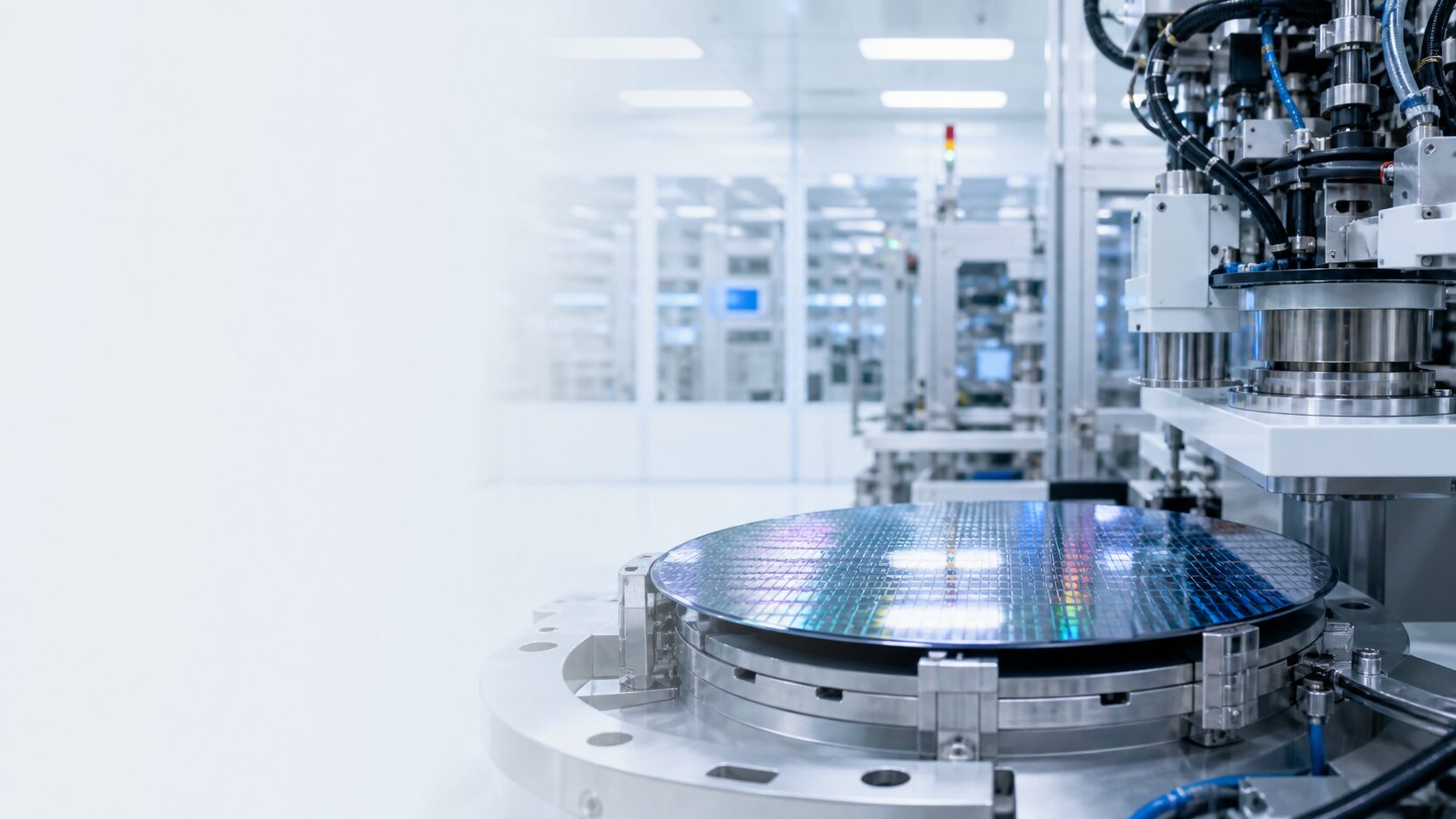
Shin-Etsu Chemical supplies semiconductor silicon and a broad range of electronic materials, including photoresists, photomask blanks, encapsulating materials, synthetic quartz products and other high-purity materials. Its semiconductor activities sit within a larger portfolio spanning electronics, infrastructure and functional materials.
Shin-Etsu Chemical is important because it participates at several upstream points where purity, consistency and long customer qualifications create barriers to substitution. Silicon wafers form the physical foundation of most integrated circuits, while lithography and packaging materials influence later process performance.
Technology & Products
Semiconductor silicon
High-purity silicon wafers used as substrates for integrated circuits.
Photoresists
Lithography materials used to transfer circuit patterns.
Photomask blanks
Starting materials for masks used in semiconductor exposure.
Synthetic quartz
High-purity optical and process materials.
Encapsulation materials
Materials used to protect semiconductor devices and packages.
Specialty electronic materials
Additional products serving fabrication and packaging workflows.
Position in the Supply Chain
The company’s semiconductor portfolio spans the substrate, lithography and packaging layers of the value chain. That breadth provides exposure to both wafer-volume growth and increasing material specifications at advanced nodes.
Strategic Position
Scale, materials science, process discipline and customer qualification support Shin-Etsu Chemical’s position. Its diversified portfolio can absorb cycles better than a single-product supplier, although major wafer capacity investments remain capital intensive.
Ecosystem Impact
Shin-Etsu supports device makers, foundries, mask producers and packaging companies. Its production also depends on energy, high-purity inputs, specialized equipment, logistics and long-term quality control across a global manufacturing network.
Outlook
Growth Drivers
- Long-term semiconductor wafer demand
- Higher purity and flatness requirements
- Advanced lithography material needs
- Packaging and thermal-management innovation
Risks
- Capital intensity and utilization cycles
- Energy and raw-material costs
- Customer inventory corrections
- Technology substitution and qualification risk
Key Points to Watch
- Semiconductor silicon capacity and utilization
- Electronic-material product mix
- Advanced-node qualification
- Capital spending and return discipline
Official Sources
Editorial note: This independent profile is based primarily on company-published information. Business conditions, products and plans may change. SemiStructure is not affiliated with the company, and this page does not constitute investment advice.
Have information about Shin-Etsu Chemical?
SemiStructure welcomes official corrections, company updates, partnership proposals, interview requests and semiconductor-industry research inquiries in English.