Lasertec
An applied-optics specialist focused on semiconductor inspection and measurement, including demanding mask-related workflows for advanced lithography.
Company Snapshot
- Founded
- 1960
- Headquarters
- 2-10-1 Shin-yokohama, Kohoku-ku, Yokohama, Kanagawa 222-8552, Japan
- Capital
- ¥931 million
- Latest net sales
- ¥251.477 billionFY ended June 2025, consolidated
- Primary focus
- Semiconductor inspection and metrology
- Value-chain position
- Masks, mask blanks and wafer inspection
Head Office
2-10-1 Shin-yokohama, Kohoku-ku, Yokohama, Kanagawa 222-8552, Japan
Manufacturing Sites
- Kanagawa — Yokohama City, Tsuzuki Ward (Lasertec Innovation Park; development and production hub)
Company Overview
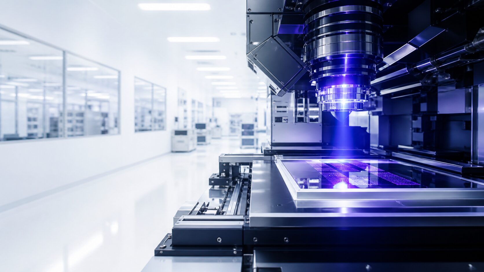
Lasertec develops inspection and measurement systems based on applied optics. Its semiconductor-related products cover mask blanks, photomasks and wafers, while the company also supplies flat-panel-display inspection systems and laser microscopes.
Lasertec demonstrates how a focused Japanese specialist can occupy a highly valuable position in a narrow process bottleneck. Inspection does not directly create a circuit, but it protects the economics of every downstream step by identifying defects before they become expensive yield losses.
Technology & Products
Mask blank inspection
Detection of defects before circuit patterns are written on a mask.
Photomask inspection
Process control for masks used in semiconductor lithography.
EUV-related inspection
Optical systems addressing leading-edge lithography requirements.
Wafer inspection
Solutions for wafer edges, films, thickness and surface conditions.
SiC wafer inspection
Inspection applications for compound and power-semiconductor materials.
Laser microscopy
Applied-optics platforms for R&D and quality control.
Position in the Supply Chain
Lasertec sits upstream of wafer patterning and at multiple wafer-control points. Its systems combine light sources, optical design, precision motion, detection, image processing and defect classification, making multidisciplinary engineering central to product performance.
Strategic Position
The company’s position is strengthened by proprietary applied-optics capabilities and products addressing difficult inspection problems. This focus can create high barriers to entry, but it can also increase dependence on a limited number of leading-edge customers and technology transitions.
Ecosystem Impact
Lasertec draws on Japanese strengths in optics, precision stages, sensors, specialty glass, vibration control and high-performance computing. Its products also support material suppliers and mask makers as well as device manufacturers.
Outlook
Growth Drivers
- EUV adoption and tighter mask-defect requirements
- Rising wafer value and yield sensitivity
- New materials and three-dimensional structures
- Growth in SiC and advanced wafer inspection
Risks
- Concentration in specialized products and customers
- Long qualification and order-recognition cycles
- Alternative inspection technologies
- Export restrictions and leading-edge investment volatility
Key Points to Watch
- EUV mask-related product adoption
- Wafer-inspection portfolio expansion
- Customer concentration
- Research spending and new-product qualification
Official Sources
Editorial note: This independent profile is based primarily on company-published information. Business conditions, products and plans may change. SemiStructure is not affiliated with the company, and this page does not constitute investment advice.
Have information about Lasertec?
SemiStructure welcomes official corrections, company updates, partnership proposals, interview requests and semiconductor-industry research inquiries in English.