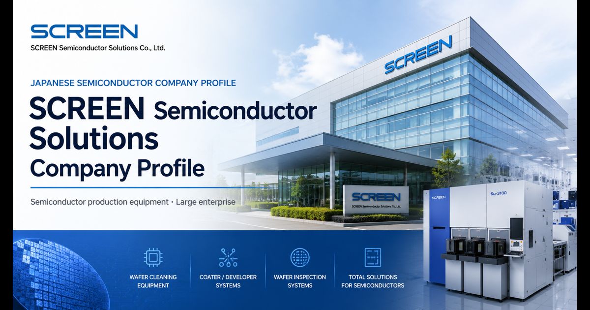
Company Snapshot
- Founded
- 2006
- Headquarters
- Tenjinkita-machi 1-1, Teranouchi-agaru 4-chome, Horikawa-dori, Kamigyo-ku, Kyoto 602-8585, Japan
- Capital
- ¥310 million
- Latest net sales
- ¥485.9 billionFY ended March 2026, SCREEN SPE segment
- Primary focus
- Wafer cleaning and surface processing
- Value-chain position
- Front-end fabrication equipment
Head Office
Tenjinkita-machi 1-1, Teranouchi-agaru 4-chome, Horikawa-dori, Kamigyo-ku, Kyoto 602-8585, Japan
Manufacturing Sites
- Shiga — Hikone City (Hikone Site)
- Shiga — Taga Town (Taga Site)
- Shiga — Yasu City (Yasu Site)
- Kyoto — Kyoto City, Fushimi Ward (Rakusai Site)
- Kyoto — Kumiyama Town (Kumiyama Site)
Company Overview
SCREEN Semiconductor Solutions develops equipment used across semiconductor wafer fabrication, including cleaning, coat/develop, thermal processing, measurement and inspection. It operates within the SCREEN Group and inherits a long industrial history in image processing, precision engineering and production equipment.
SCREEN’s strategic importance comes from the frequency of cleaning and surface-preparation steps across a semiconductor process flow. As device structures become smaller and more three-dimensional, removing particles and residues without damaging sensitive surfaces becomes more difficult and more valuable.
Technology & Products
Single-wafer cleaning
High-throughput cleaning and surface preparation for advanced wafer processes.
Batch cleaning
Processing platforms for multiple wafers and established production flows.
Coat and develop
Photoresist coating and development systems supporting lithography.
Thermal processing
Annealing and related systems used to control wafer properties.
Measurement and inspection
Process-control equipment for identifying defects and variation.
Advanced packaging
Lithography and processing solutions for packaging applications.
Position in the Supply Chain
SCREEN sits at the process-control boundary between chemistry, equipment engineering and yield management. Its tools interact with high-purity chemicals, ultrapure water, wafer-handling automation and factory-control systems, making qualification and service capability important parts of the customer relationship.
Strategic Position
The company benefits from an installed base and technical knowledge accumulated across multiple cleaning architectures. Its competitive position depends on process performance, productivity, chemical efficiency, defect control and the ability to support customers as structures and materials change.
Ecosystem Impact
SCREEN creates demand for precision components, fluid-control systems, pumps, filters, chemical-delivery equipment, sensors and maintenance services. Its position also makes it an important channel through which Japanese component suppliers participate in global fabs.
Outlook
Growth Drivers
- More cleaning steps in advanced logic and memory processes
- Growth in power semiconductors and mature-node capacity
- Higher contamination-control requirements
- Advanced-packaging process expansion
Risks
- Cyclical wafer-fab equipment spending
- Qualification delays and concentrated customers
- Competition in major process-equipment categories
- Export controls and regional supply-chain constraints
Key Points to Watch
- Order trends and fab-investment timing
- Progress in advanced cleaning applications
- Service and installed-base expansion
- Exposure to power semiconductor and packaging demand
Official Sources
Editorial note: This independent profile is based primarily on company-published information. Business conditions, products and plans may change. SemiStructure is not affiliated with the company, and this page does not constitute investment advice.
Have information about SCREEN Semiconductor Solutions?
SemiStructure welcomes official corrections, company updates, partnership proposals, interview requests and semiconductor-industry research inquiries in English.