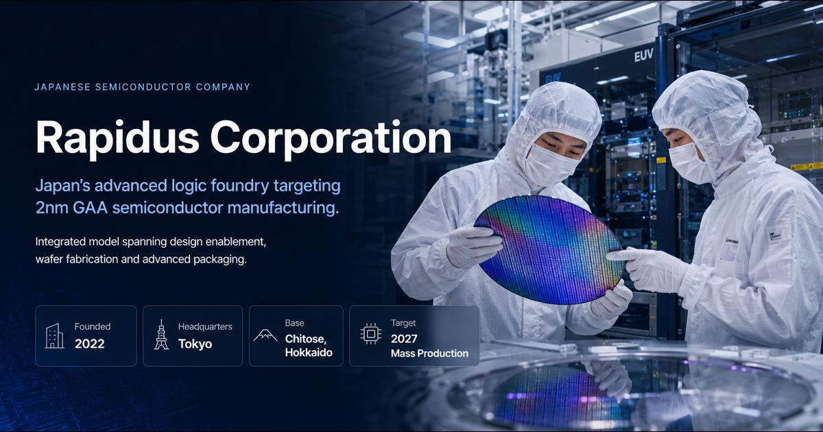
Company Snapshot
Head Office
Kojimachi Diamond Building, 4-1 Kojimachi, Chiyoda-ku, Tokyo 102-0083, Japan
Manufacturing Sites
- Hokkaido — Chitose City (IIM-1, 758-62 Bibi)
- Hokkaido — Chitose City (Rapidus Chiplet Solutions, 758-173 Bibi)
Company Overview
Rapidus Corporation is a Japanese semiconductor manufacturer established in 2022 to develop and manufacture advanced logic semiconductors. The company is building a foundry business centered on a 2nm-generation Gate-All-Around process and aims to connect semiconductor design, front-end wafer fabrication and advanced packaging within a more integrated manufacturing model.
Rapidus is positioned differently from Japanese semiconductor companies focused primarily on mature process nodes, memory, power semiconductors or vertically integrated device businesses. Its strategic objective is to establish domestic capability in leading-edge logic manufacturing and provide an additional advanced foundry option for global semiconductor customers.
SEMISTRUCTURE VIEW
Rapidus occupies a distinctive position in Japan’s semiconductor value chain. Its strategy is not limited to building a 2nm fabrication facility. The company is attempting to connect design enablement, front-end processing and advanced packaging while shortening the cycle between semiconductor design and manufacturing.
Technology & Manufacturing
Rapidus is developing a technology platform centered on advanced logic manufacturing, design-manufacturing optimization and next-generation packaging. The company places particular emphasis on reducing development lead times and improving the flow of manufacturing data back into semiconductor design.
2nm-generation GAA
Leading-edge logic process technology based on Gate-All-Around transistor architecture.
RUMS
Rapidus Unified Manufacturing Service, intended to integrate design support, front-end manufacturing and back-end processing.
Raads
AI-assisted design technologies intended to support semiconductor design optimization.
DMCO
Design-manufacturing co-optimization intended to improve coordination between semiconductor design and production processes.
Single-wafer Processing
A manufacturing approach intended to support detailed process data collection and flexible production.
Advanced Packaging
Development areas include chiplet integration, 3D integration and panel-level packaging.
IIM — Chitose, Hokkaido
Rapidus is developing IIM, Innovative Integration for Manufacturing, as its advanced semiconductor research and manufacturing base in Chitose, Hokkaido.
According to Rapidus, the pilot line began operation in April 2025, with mass production targeted for 2027. The site is central to the company’s effort to establish domestic Japanese manufacturing capability for leading-edge logic semiconductors.
The Chitose project is also important beyond Rapidus itself. The establishment of a leading-edge semiconductor manufacturing base has the potential to attract semiconductor equipment suppliers, materials companies, infrastructure providers, logistics companies and engineering talent to Hokkaido.
- Facility
- IIM — Innovative Integration for Manufacturing
- Location
- Chitose, Hokkaido, Japan
- Role
- Advanced semiconductor R&D and manufacturing
- Pilot Line
- Operating since April 2025
- Mass Production
- Targeted for 2027
Strategic Position
Rapidus represents one of Japan’s most significant attempts to rebuild domestic capability in leading-edge semiconductor manufacturing.
Japan remains globally important in semiconductor manufacturing equipment, materials, silicon wafers, specialty chemicals, power semiconductors and selected device categories. Its position in advanced logic fabrication, however, declined significantly over several decades.
Rapidus is therefore strategically important not only as an individual semiconductor company but also as part of Japan’s broader effort to strengthen economic security, semiconductor supply-chain resilience and domestic advanced manufacturing capability.
If the company can establish a qualified 2nm process, achieve commercially viable yields and secure sufficient customer demand, Rapidus could become an additional manufacturing option for companies developing AI processors, high-performance computing devices, automotive semiconductors and application-specific logic.
Ecosystem Impact
Rapidus could also have a broader impact on Japan’s semiconductor ecosystem. Leading-edge manufacturing requires a dense network of equipment, materials, infrastructure and engineering suppliers.
Areas potentially affected by Rapidus’ expansion include lithography-related technologies, deposition and etching equipment, cleaning systems, inspection and metrology, specialty chemicals, high-purity gases, silicon wafers, photomasks, advanced substrates, packaging technologies, cleanroom infrastructure and factory automation.
The concentration of these activities around Hokkaido may gradually create a semiconductor cluster extending beyond the Rapidus manufacturing site itself.
Outlook
The strategic rationale for Rapidus is supported by structural demand for advanced computing and growing interest in geographically diversified semiconductor manufacturing. At the same time, leading-edge foundry development involves unusually high technical, financial and commercial execution requirements.
Growth Drivers
- Long-term expansion of AI and high-performance computing
- Demand for lower-power advanced logic semiconductors
- Growth of application-specific semiconductor designs
- Expansion of chiplet and heterogeneous integration architectures
- Demand for geographic diversification in semiconductor manufacturing
- Japan’s established semiconductor equipment and materials ecosystem
Execution Risks
- Qualification of the 2nm-generation process
- Yield improvement and manufacturing stability
- Customer acquisition and volume-production commitments
- Large and continuing capital expenditure requirements
- Access to advanced tools, materials and semiconductor IP
- Recruitment and development of engineering talent
- Transition from pilot production to economically viable volume manufacturing
Key Milestones
Rapidus’ long-term position will depend less on the announcement of individual technology milestones than on its ability to move from development into repeatable commercial manufacturing.
-
2nm process qualification
Progress in process development and customer qualification will be a central indicator of technological readiness. -
Yield ramp
Improving yield to commercially sustainable levels will be critical to manufacturing economics. -
Customer commitments
The transition from development partnerships to meaningful production customers will be an important commercial milestone. -
Advanced packaging integration
The ability to combine leading-edge logic with chiplet and 3D packaging capabilities could become a source of differentiation. -
2027 volume-production transition
The move from pilot operations toward stable mass production will be one of the most important execution tests for the company.
Official Sources
Editorial note: This independent company profile is based primarily on information published by Rapidus and other publicly available sources. Future technology plans, investment programs and production schedules may change. SemiStructure is not affiliated with Rapidus Corporation, and this page does not constitute investment advice.
Have information about Rapidus?
SemiStructure welcomes company-information updates, corrections, partnership proposals, interview requests and semiconductor industry research inquiries in English.