TOWA Corporation
A Kyoto-based semiconductor-packaging specialist known for molding equipment, singulation systems and ultra-precision molds.
Company Snapshot
- Founded
- 1979
- Headquarters
- 5 Kamichoshi-cho, Kamitoba, Minami-ku, Kyoto-shi, Kyoto 601-8105, Japan
- Capital
- ¥8.986 billion
- Latest net sales
- ¥54.365 billionFY ended March 2026, consolidated
- Primary focus
- Molding and singulation equipment
- Value-chain position
- Back-end and advanced packaging
Head Office
5 Kamichoshi-cho, Kamitoba, Minami-ku, Kyoto-shi, Kyoto 601-8105, Japan
Manufacturing Sites
- Kyoto — Kyoto City, Minami Ward (Headquarters / Factory)
- Kyoto — Uji City (Kyoto East Plant)
- Saga — Tosu City (Kyushu Works)
Company Overview
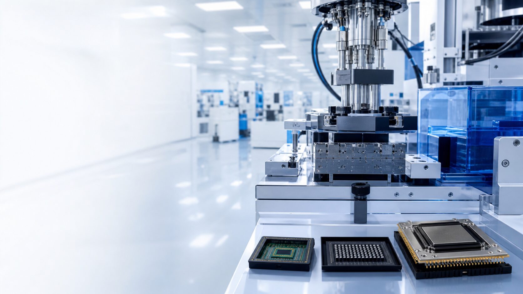
TOWA develops semiconductor manufacturing equipment and precision molds centered on resin-sealing and package processing. Its portfolio includes transfer and compression molding, singulation equipment, tooling and related services used in conventional and advanced packaging.
TOWA is a useful example of a mid-sized Japanese specialist holding a critical global position in the back end. Molding protects devices and influences reliability, package shape and production yield; the equipment and mold must work as one process system.
Technology & Products
Compression molding
Resin-sealing systems for wafers, panels and advanced package formats.
Transfer molding
Production equipment for established semiconductor package processes.
Singulation
Systems that separate molded packages into individual units.
Ultra-precision molds
Tooling engineered together with packaging equipment.
Laser processing
Capabilities supporting package marking and precision processing.
Service and connected support
Maintenance, tooling and production-support offerings.
Position in the Supply Chain
TOWA operates after wafer fabrication, where individual dies or wafer-level structures are protected and prepared for use in electronic systems. Its equipment interacts with mold compounds, substrates, leadframes, wafers, panels and factory automation.
Strategic Position
The combination of molding equipment and precision molds creates process knowledge and customer switching costs. Advanced packaging expands opportunities but requires continued development for larger formats, warpage control, thin structures and heterogeneous integration.
Ecosystem Impact
TOWA connects resin and encapsulation suppliers, substrate makers, precision tooling, laser processing, handling automation and outsourced assembly and test companies. Its equipment can therefore serve as a bridge between Japanese materials strengths and global packaging investment.
Outlook
Growth Drivers
- Advanced packaging and heterogeneous integration
- Wafer- and panel-level molding
- Power modules and larger package formats
- Demand for automation and yield control
Risks
- Back-end capital-spending cycles
- Packaging-architecture transitions
- Customer qualification and project timing
- Competition in molding and singulation equipment
Key Points to Watch
- Compression-molding adoption
- Advanced-packaging order mix
- Mold and service contribution
- Expansion beyond conventional package formats
Official Sources
Editorial note: This independent profile is based primarily on company-published information. Business conditions, products and plans may change. SemiStructure is not affiliated with the company, and this page does not constitute investment advice.
Have information about TOWA Corporation?
SemiStructure welcomes official corrections, company updates, partnership proposals, interview requests and semiconductor-industry research inquiries in English.